Monday, February 29, 2016

Week 8


Week 8 Rube Goldberg 

In our Rube Goldberg machine we will combine several circuits we used in previous weeks to combine a digital display, motor, relay, opamp, temperature sensor, and a LED to hit a ball off a tee.
In our set up we have our clock sending a signal to our counter; the then counter is sending a signal to the driver, then the driver controlling the digital display. The display will continue to count from 0 to 9, once it past 9 it will start over.

Whole circuit, and setup


We connected the inputs of a XOR gate to the C and D outputs of the counter. Then we connect an LED to the output of the XOR gate to show when the logic gate runs true. The logic gate will run true when the display is between 4 and 9.
From the truth table and the table of the outputs of the counter you can see the green LED will be on when the display if between 4 and 9. Between 4 and 9 either the D or C input is high, but never both at the same time.
XOR Gate(7486) Truth Table 
Truth Table for the counter

In the picture below you can see that the display is not between 4 and 9 and the green LED is not on.
Figure 2: Display 3,green LED not on


As you can see in the picture below the display is now between 4 and 9 and the green LED is on.
Figure 3: Display between 4 and 9, green LED on

We have a blue LED connected to the normally closed terminal of the relay, so it will be on when the relay is not engaged. 
Figure 4: Relay not engaged, blue LED on
We have connected a clear LED to the normally open terminal of the relay to show when the relay is engaged for testing. When we engage the relay you can see the clear LED come on and the blue LED go off. In the photo we manually changed the relay by applying 6 volts to the solenoid for testing purposes.
Figure 5: Relay engaged, blue LED off, and clear LED on
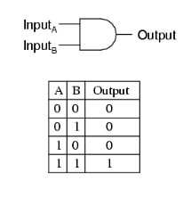
We now have connected the output of the XOR gate and the output of the normally closed terminal of the relay to a AND gate. The output out of the AND gate is connected to the yellow LED light to represent out motor. Following the truth table for the AND gate below you can see that the yellow LED will turn on when both the relay and the XOR gate run true.
AND Gate (7408) Truth Table

In the photo below you can see clear LED is on showing that the relay is engaged, but the green light is not on showing that the XOR gate is now true. Which doesn’t turn on the yellow LED.
Figure 6: Relay engaged, clear LED on, green and yellow LED off
Now when the display is between 4 and 9 the green LED turns on, this make the logic for the and gate run true turning on the yellow LED.
Figure 7: Relay engaged, display between 4 and 9, green, clear and yellow light on.
We connected the temperature sensor to the op-amp in a non-inventing configuration. Then the amplified signal will go to the solenoid of the relay. When the temperature sensor is heated with the blow dryer it will engage the relay.


In the video below you will see the whole circuit in motion. The display will repeatedly count from 0 to 9, the Green LED will be on from 4 to 9 on the display, the relay will engage when the temperature sensor is warm enough, the motor will spin once the green LED is on and the relay are both engaged. The motor will then send the ping pong ball flying.

Problems we had
We first notice that the display was counting too fast for our setup, so we had to reconfigure the set up of the resistors on the clock to slow the clock speed down. We increased Ra from 150k ohms to 330 ohms. Then we increase Rb to 820k ohms. Below you can see out clock set up.

We had an issue with the AND gate running true with only one input of 1, from the truth table of an AND gate we know this is not right. We found that the one input of the AND gate that was not one need to be ground to the AND gate to function properly. So we ground the inputs, but this caused and issue since electricity is lazy and flowed the path of least resistance and with the inputs grounded the signals coming from the relay and the XOR gate would go straight to ground. So we instead of directly grounding the inputs we used a 1k ohm resistor to ground them. This then forced the signals to go to  the AND gate and not straight to ground.
The last issue we had was that we found the output of the AND gate was not strong enough to power the motor. So we thought about the first time we built a Rube Goldberg circuit with a transistor and the light sensor. We used the same set up but replaced the photocell and the 5 v supply with the output of the AND gate, thus allowing us to turn the motor with an AND gate.

Friday, February 26, 2016

Week 7

Blogsheet week 7
Digital Circuits
1.       Force sensing resistor gives a resistance value with respect to the force that is applied on it. Try different loads (Pinching, squeezing with objects, etc.) and write down the resistance values. (EXPLAIN with TABLE)
Table 1. Force sensing resistor values with different loads
 
      When there is no load on the force sensing resistor, the resistor value will be very large (out of limit), and if we put more load on the force sensing resistor, then the resistor value will decrease.
2.       7 Segment display:
a.       Check the manual of 7 segment display. Pdf document’s page 5 (or in the document page 4) circuit B is the one we have. Connect pin 3 or pin 14 to 5 V. Connect a 330 Ω resistor to pin 1. Other end of the resistor goes to ground. Which line lit up? Using package dimensions and function for B (page 4 in pdf), explain the operation of the 7 segment display by lighting up different segments. (EXPLAIN with VIDEO).


Video 1. Operation of the 7 segment display

        If we connect a 330 Ω resistor to pin 1, and the other end of the resistor goes to ground, then the top line will light up. If we connect different pins to the ground, then different segments will be lighted up.

Figure 1. Design of 7-segment
b.      Using resistors for each segment, make the display show 0 and 5. (EXPLAIN with PHOTOs)


Figure 2. Display of 5


Figure 3. Display of 0


      As Figure 1 shows, pin 3 or 14 need to connect to the power supply, and if we want to show 5, then we need to ground pin 1, 2, 8, 10, 11; if we want to show 0, then we need to ground 1, 2, 7, 8, 10, 13.


3.       Display driver (7447). This integrated circuit (IC) is designed to drive 7 segment display through resistors. Check the data sheet. A, B, C, and D are binary inputs. Pins 9 through 15 are outputs that go to the display. Pin 8 is ground and pin 16 is 5 V.
a.       By connecting inputs either 0 V or 5 V, check the output voltages of the driver. Explain how the inputs and outputs are related. Provide two different input combinations. (EXPLAIN with PHOTOs and TRUTH TABLE)

UPDATE! You cannot actually measure the output voltages directly (I challenge you to figure out why!). You need to connect an LED and a resistor. LED’s positive terminal will go to 5 V. Negative terminal will be connected to your outputs via a resistor. The circuit would look like below:


Figure 4. Display of 0 with driver

Figure 5. Display of 4 with driver
Table 2. Truth table for display 0 and 4
Table 3. Function table


      7447 display driver will transfer binary coded decimals to output signals to drive the 7-segment display. Table 3 shows how the binary codes can be transferred to number displays. We choose input combination D-0, C-0, B-0, A-0, and it will give us 0 on the 7-segment display; then we choose input combination D-0, C-1, B-0, A-0, and it will give us 4 on the 7-segment display.


b.      Connect the display driver to the 7 segment display. 330 Ω resistors need to be used between the display driver outputs and the display (a total of 7 resistors). Verify your question 3a outputs with those input combinations. (EXPLAIN with VIDEO)
Video 2. Verify the outputs with different input combinations


Both 2 outputs of 3a can be verified.

4.       555 Timer:
a.       Construct the circuit in Fig. 14 of the 555 timer data sheet. VCC = 5V. No RL (no connection to pin 3). RA = 150 kΩ, RB = 300 kΩ, and C = 1 µF (smaller sized capacitor). 0.01 µF capacitor is somewhat larger in size. Observe your output voltage at pin 3 by oscilloscope. (Breadboard and Oscilloscope PHOTOs)

Figure 6. The circuit of 555 timer

Figure 7. Oscilloscope display of pin 3's voltage
Figure 7 shows the output voltage at pin 3, and the frequency is about 3Hz. As you can see the clock puts out a constant signal.

b.      Does your frequency and duty cycle match with the theoretical value? Explain your work.


Table 4. Frequency and theoretical
 From the oscilloscope, we can see that the measured frequency is 3Hz, and the duty cycle is about 0.33. From the calculation, we know that the theoretical frequency value is
and the theoretical duty cycle is 


c.       Connect the force sensing resistor in series with RA. How can you make the circuit give an output? Can the frequency of the output be modified with the force sensing resistor? (Explain with VIDEO)


Video 3. Connect 555 with force sensing resistor


     The force sensing resistor is like a trigger, if we press (put load on) the force sensing resistor, then we can make the circuit give an output. Also, we can adjust the frequency of the output by pressing the force sensing resistor with different paces.

5.       Binary coded decimal (BCD) counter (74192). This circuit generates a 4-bit counter. With every clock change, output increases; 0000, 0001, 0010, …, 0111, 1000, 1001. But after 1001 (which is decimal 9), it goes back to 0000. That way, in decimal, it counts from 0 to 9. Outputs of 74192 are labelled as QA (Least significant bit), QB, QC, and QD (Most significant bit) in the data sheet (decimal counter, 74192). Use the following connections:
5 V: pins 4, 11, 16.
0 V (ground): pins 8, 14.
10 µF capacitor between 5 V and ground.
a.       Connect your 555 timer output to pin 5 of 74192. Observe the input and each output on the oscilloscope. (EXPLAIN with VIDEO and TRUTH TABLE)


Video 4. Connect 555 to 74192


Table 5. Truth table
     By observing the outputs on the oscilloscope, we can see that the outputs of QA changes faster than QB than QC than QD, and this result can be supported by table 5.


6.       7486 (XOR gate). Pin diagram of the circuit is given in the logic gates pin diagram pdf file. Ground pin is 7. Pin 14 will be connected to 5 V. There are 4 XOR gates. Pins are numbered. Connect a 330 Ω resistor at the output of one of the XOR gates.
a.       Put an LED in series to the resistor. Negative end of the LED (shorter wire) should be connected to the ground. By choosing different input combinations (DC 0V and DC 5 V), prove XOR operation through LED. (EXPLAIN with VIDEO)


Video 5. Prove XOR operation through LED

Table 6. Truth table of XOR

     According to table 6, we should get LED on when input as A-0 & B-1 or A-1 & B-0, and the LED should off when both inputs are 0 or 1. These combinations all be verified in the video 5.

b.      Connect XOR’s inputs to the BCD counters C and D outputs. Explain your observation. (EXPLAIN with VIDEO)
 
Video 6: XOR gate with inputs of C and D of counter and LED connected to the output. 


      If the combination is input A-0, B-1 or A-1, B-0, then the LED will be on. 

c.     For 6b, draw the following signals together: 555 timer (clock), A, B, C, and D outputs of 74192, and the XOR output. (EXPLAIN with VIDEO)
      In the video below we explain the how the outputs of the clock set the pace for the counter and the the XOR operates off the outputs of the C and D outputs of the counter. The truth table in the video is just to show the operation of the XOR, not to show that A and B are controlling the XOR in our experiment.


Video 7: Signals of Clock, Counter, and XOR gate

7.       Connect the entire circuit: Force sensing resistor triggers the 555 timer. 555 timer’s output is used as clock for the counter. Counter is then connected to the driver (Counter’s A, B, C, D to driver’s A, B, C, D). Driver is connected to the display through resistors. XOR gate is connected to the counter’s C and D inputs as well and an LED with a resistor is connected to the XOR output. Draw the circuit schematic. (VIDEO and PHOTO)


Video 8. The operation of entire circuit
                

The video shows the operation for the entire circuit.

Figure 8: Schematic of the circuit with a XOR gate.
Figure 9: Full circuit controlled by force sensor


8.       Using other logic gates provided (AND and OR), come up with a different LED lighting scheme. (EXPLAIN with VIDEO)


Video 9. AND gate


Video 10. OR gate


Table 5. Truth tables of AND and OR gates

      First we use AND gate, and the inputs are A and B of the counter. According to table 3, LED can be turned on when the counter shows 3 or 7 (because when display shows 3 or 7, it means both inputs A and B are high), and other numbers the LED can not be turned on.

      Second we use OR gate, and the inputs are still A and B of the counter. According to table 3, LED can not be turned on when the counter shows 0, 4 or 8 (because when display shows 0, 4 or 8, it means both inputs A and B are low), and other numbers the LED will be on.